Semiconductors and power electronics
Semiconductor education and partnerships
ASU’s unique semiconductor processing certificate offers strategic training in multiple aspects of chip production including semiconductor manufacturing, processing, packaging and characterization. Faculty, researchers, students and industry collaborate at ASU’s elite semiconductor research facilities where an emphasis on industry-relevant research has forged mutually beneficial partnerships with local semiconductor firms.
Research and development labs
- MacroTechnology Works is a unique facility that allows ASU to advance research in partnership with private industry. The facility offers clean rooms, wet labs, dry labs, high bay space and office accommodations.
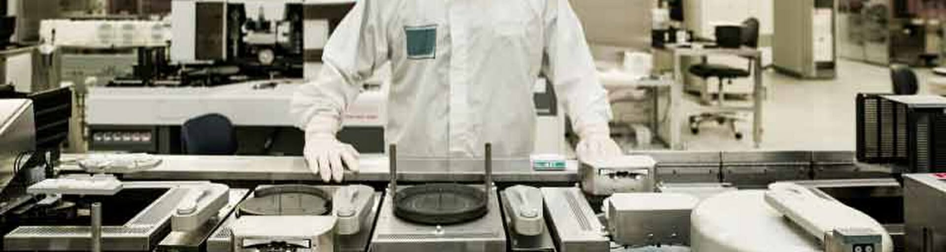
- ASU NanoFab is a flexible nanoscale processing and fabrication facility at Arizona State University offering state-of-the-art device processing and characterization tools for university research and external company prototype development.
- Eyring Materials Center provides academic and industry researchers
with open access to advanced facilities and equipment for materials characterization; surface, optical and structural analysis; and high-resolution electron microscopy.
The ASU advantage
Collaboration and innovation thrive in ASU’s robust centers, programs and state-of-the-art facilities.
Students gain critical experience through hands-on learning and research, and companies have access to a pipeline of technical talent emerging from ASU.
Manufacturing the future
Funded by the NSF, ASU faculty are developing a method
for metal-assisted, electrochemical nanoimprinting, or Mac-Imprint, that can be used to manufacture the tiny, complex nanoscale semiconductor devices of the future.
AZNext is a public-private partnership designed to create a bold, innovative and sustainable workforce development ecosystem that addresses the need for more skilled workers.
This ASU research lab focuses on wide band-gap, device-based, advanced power electronics for the
application of:
- Medium voltage motor drives.
- Electric vehicles.
- PV grid integration.
- Data center power conversion.
This research lab is sponsored by the National Science Foundation, Department of Energy SETO, Infineon, ON Semiconductor, Hitachi, SRP, ULC Robotics and more.
Advancing partnerships for prosperity
ASU pulls in big ideas from industry for translation into high-impact products, inventions and services — creating a feedback loop between market needs, research, education and commercial application.
As part of Arizona’s New Economy Initiative, ASU will create five new Science and Technology Centers, two of which will contribute to the microelectronics industry.
- Energy Materials and Devices Center.
- Advanced Manufacturing Center.
The STCs will serve as robust hubs for collaboration and innovation.
ASU offers a unique degree certificate in semiconductor processing
Applied Materials, a California-based materials engineering company, leases space at ASU’s MacroTechnology Works for research and development support, hires from the ASU talent pipeline and partners with ASU semiconductor experts

Semiconductors and power electronics
Download a printable version of this webpage.
Get in touch with questions and comments
ASU Economic Development is here to be your partner, your resource and your advocate. Contact us today for a personal consultation.